M.U. SEM Facility
.
 |
||||
M.U. SEM Facility |
||||
. |
||||
| .
|
|
 |
 |
|||||||
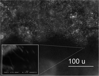
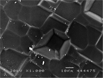
| A bundle of single walled nanotubes with a couple of tubes sticking out in the zoomed view. | Thin diamond films deposited on silicon by Dr. Vasheesta and students. | ||||||||
|
|
|
 |
||||||
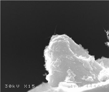
| Also thin diamond films deposited on silicon by Dr. Vasheesta and students. Here we can also see some glass nodules formed in the high temp. process. | As part of a capstone study, we applied some of the single walled nanotubes to an AFM tip and succesfully imaged with it. Note the very fine tube protruding from the ‘course’ (1um) tip | ||||||||
 |
|||||||||
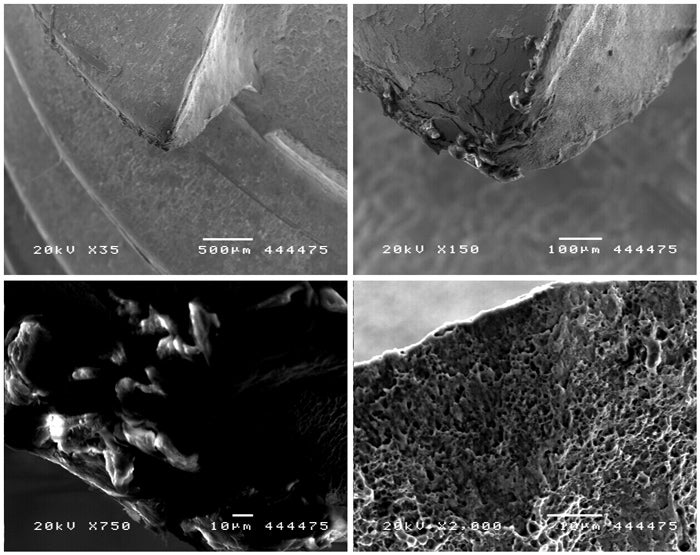
WV honors academy students (high school). Did this fracture analysis of machined (above) and cast (below) alloys. |
|||||||||
 |
|||||||||
|
|||||||||
|
|||||||||
|
|||||||||